
HARDWARE DESIGN REVIEW, LAYOUT, ANALYSIS, FABRICATION AND ASSEMBLY LEVEL SOLUTIONS:
Followings are the have been provided by TECHNID SOLUTIONS as a Board Level Solution from after Circuit Design Review from draft designs provided by the customer:-
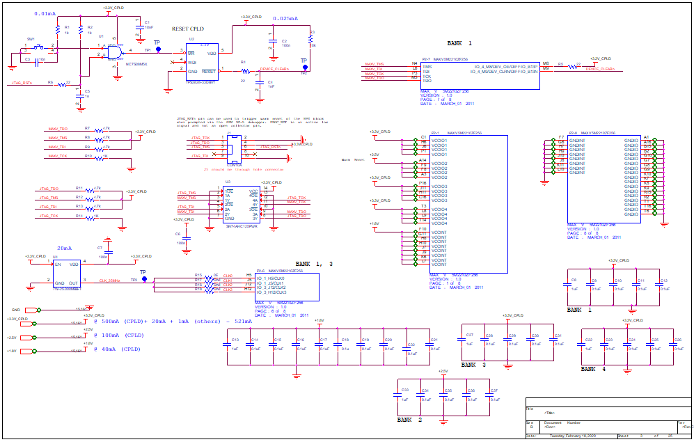
- FPGA based SPI bus based CPU Card for controlling all the IO Cards via the Back Plane Card and passing important interface for Nuclear Reactor Application.
- FPGA based 66MHz cPCI bus Back Plane Card used for holding the CPU card and the IO cards used for Nuclear Reactor Applications.
- FPGA based 66MHz cPCI bus Leak Detector Card used for detecting the leakage in Coolant Pipes in Nuclear Reactor Vessel in Nuclear Reactor Application.
- FPGA based 66MHz cPCI bus Optical Encoder Card used for remotely reading and processing the value of Optical Encoders over RS422 bus in Nuclear Reactor Application.
- FPGA based 66MHz cPCI bus Thermocouple Card used for reading data from 16 Thermocouples used to measure the temperature difference across the coolant pipes in the Nuclear Reactor Vessel in Nuclear Reactor Application.
- FPGA based 66MHz cPCI bus Analog IO Card used for reading Analog Input and generating Analog Output Data used in Nuclear Reactor Application.cPCI based Remote Terminal Unit Card and Board Tester Card to be used in Conjunction with Analog IO Card used in Nuclear Reactor Application.
- ATMEGA Controller based Remote Terminal Unit Card used for reading isolated Thermocouple data used Nuclear Reactor Application
- 1.5 Million Gate based General Purpose Actel FPGA based Kit designed for developing hands on expertise on the FPGA based design and development.
We provide error free design to the customer so that their solutions run in one single attempt and that is the USP of TECHNID SOLUTIONS.
Process Flow:
-
 1
1
Reading System Specification.
-
 2
2
General Study of the Circuit Design for mapping the functional verification of the design with System specification.
-
 3
3
Detail Component level study through datasheets and its verification with circuit design.
-
 4
4
Current Budget and Power Budget Analysis of the Circuit Design.
-
 5
5
Circuit Design Modification based on the detail design findings with customer approvals.
-
 6
6
Detailed Layout Guideline Study of Individual components and total Board Layout Planning.
-
 7
7
Netlist Generation and Verification.
-
 8
8
BOM Generation and Component Procurement through Authorized Distributors.
-
 9
9
Layout Design and Development as per Stack Up and Generation of Release Files.
-
 10
10
SI Analysis.
-
 11
11
PI Analysis.
-
 12
12
Thermal Analysis.
-
 13
13
PCB Fabrication.
-
 14
14
PCB Assembly.
-
 15
15
Module GA Drawing.
-
 16
16
Module Fabrication.
-
 17
17
Module Assembly.
-
.png) 18
18
Board Level Testing.
-
.png) 19
19
Customer Approvals at each and every critical step.
Subscribe Newsletter
A quick message to TECHNID2
Client Speaks
Lorem Ipsum is simply dummy text of the printing and ty . . .
Lorem Ipsum is simply dummy text of the printing and ty . . .
Lorem Ipsum is simply dummy text of the printing and ty . . .