
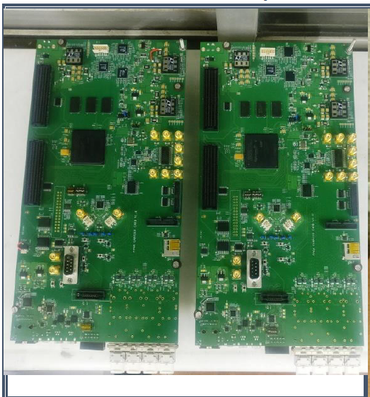
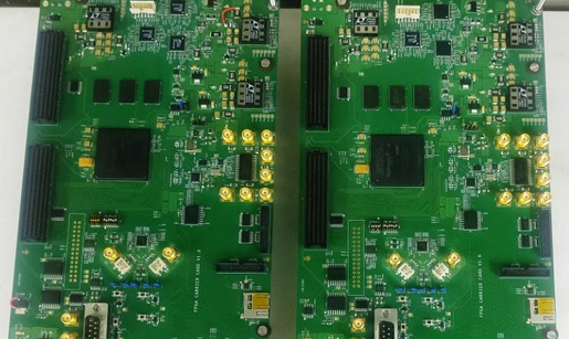
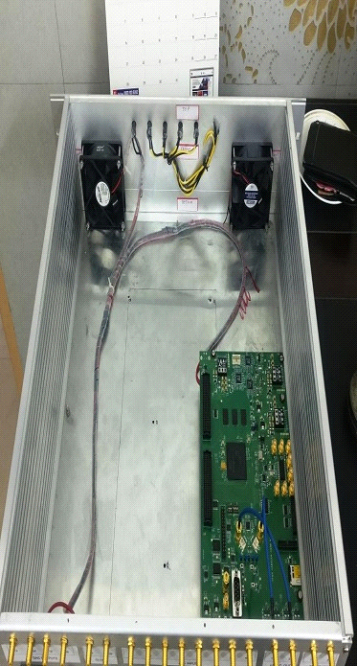
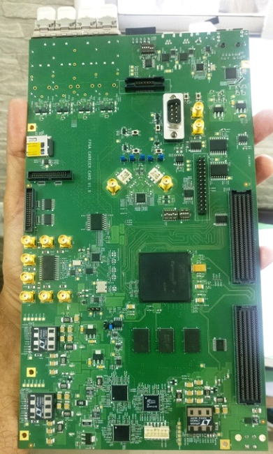
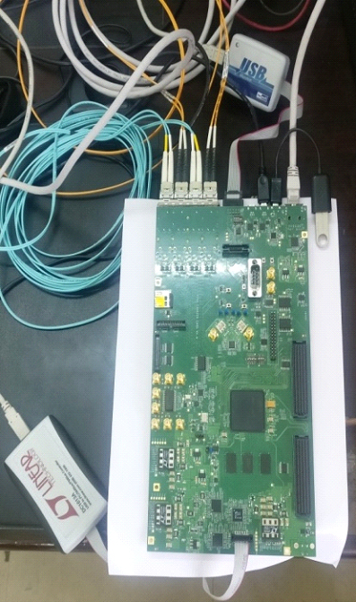
This is a CYCLONE V SX SOC based ANSI VITA electrical compliant General Purpose Base card which can be used with several mezzanine cards for various applications. Following are the features of this highly complex card:-
- High Speed, high density FPGA with 110K logic elements, 3.125Gbps transceivers (Nos. 9), integrated Dual-core hard processor system up to 800 MHz maximum frequency.
- 670 MHz clock input, 400MHz interconnect frequency with support for symmetric and asymmetric multiprocessing in 896 FBGA package with the fastest speed grade available.
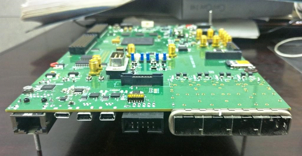
- 1 number of IEEE 802.3 based Gigabit Ethernet support using RGMII MAC compliant with 1000BASE-T specifications using CAT5 UTP cable or better.
- 4 numbers of Duplex Hot Pluggable IEEE 802.3AH based Gigabit Ethernet support compliant with 1000BASE-SX PMD Specifications, SFP SMA using Multimode Fibre up to 500m.
- Using SFP, Card acts as White Rabbit Node using SYNCE and PTP in a large network.
- ANSI VITA 57.1 based FMC connectors for interfacing with Mezzanine Ultra high speed ADC-DAC Card and other various cards using SERDES interface. Control of Mezzanine Card peripherals like ADC, DAC, Clock using SPI and I2C Control.
- Ultra low noise and sub ps jitter on board Clock generation using DAC controlled VCXO and VCO. Clock configurable between LVPECL, LVDS [625 MHz] and LVCMOS [250 MHz].
- Clock selection between ON-Board Clock generation and Clock coming from Mezzanine Card.
- 400MHz, 1Gbyte DDR3 with EEC support on HPS side.
- Accommodates boot options such as SD/MMC, QSPI using HPS.
- USB2.0 OTG Interface for transfer of data to a remote system or a storage device.
- 64Mbyte QSPI FLASH for HPS boot
- μSD slot connected to HPS for UBOOT and LINUX booting. Complete BSP has been provided for testing each and every interface.
- EEPROM for general Solid State storage, 32Kbits
- JTAG interface and MICTOR Connector for FPGA and or HPS side debugging.
- On board Very high speed 250 MSPS DAC for debugging purpose.
- On board RTC.
- 25 MHz HPS clock
- 1MHz and 50MHz clock oscillators.
- Highly advanced and extremely low noise PMBUS controlled power architecture with voltage monitors on every DC to DC Converter output in Servo Controlled Loop Mechanism.
- Test codes for all the various interfaces along with Linux boot up image.
Applications:- Low Level RF Detection in Accelerator Control Application.
Subscribe Newsletter
A quick message to TECHNID
Client Speaks
Lorem Ipsum is simply dummy text of the printing and ty . . .
Lorem Ipsum is simply dummy text of the printing and ty . . .
Lorem Ipsum is simply dummy text of the printing and ty . . .
Features
This is a CYCLONE V SX SOC based ANSI VITA electrical compliant General Purpose Base card which can be used with several mezzanine cards for various applications. Following are the features of this highly complex card:-
- High Speed, high density FPGA with 110K logic elements, 3.125Gbps transceivers (Nos. 9), integrated Dual-core hard processor system up to 800 MHz maximum frequency.
- 670 MHz clock input, 400MHz interconnect frequency with support for symmetric and asymmetric multiprocessing in 896 FBGA package with the fastest speed grade available.

Features
- 1 number of IEEE 802.3 based Gigabit Ethernet support using RGMII MAC compliant with 1000BASE-T specifications using CAT5 UTP cable or better.
- 4 numbers of Duplex Hot Pluggable IEEE 802.3AH based Gigabit Ethernet support compliant with 1000BASE-SX PMD Specifications, SFP SMA using Multimode Fibre up to 500m.
- Using SFP, Card acts as White Rabbit Node using SYNCE and PTP in a large network.
Features
- ANSI VITA 57.1 based FMC connectors for interfacing with Mezzanine Ultra high speed ADC-DAC Card and other various cards using SERDES interface. Control of Mezzanine Card peripherals like ADC, DAC, Clock using SPI and I2C Control.
- Ultra low noise and sub ps jitter on board Clock generation using DAC controlled VCXO and VCO. Clock configurable between LVPECL, LVDS [625 MHz] and LVCMOS [250 MHz].
- Clock selection between ON-Board Clock generation and Clock coming from Mezzanine Card.
Features
- 400MHz, 1Gbyte DDR3 with EEC support on HPS side.
- Accommodates boot options such as SD/MMC, QSPI using HPS.
- USB2.0 OTG Interface for transfer of data to a remote system or a storage device.
- 64Mbyte QSPI FLASH for HPS boot
- μSD slot connected to HPS for UBOOT and LINUX booting. Complete BSP has been provided for testing each and every interface.
Features
- EEPROM for general Solid State storage, 32Kbits
- JTAG interface and MICTOR Connector for FPGA and or HPS side debugging.
- On board Very high speed 250 MSPS DAC for debugging purpose.
- On board RTC.
- 25 MHz HPS clock
- 1MHz and 50MHz clock oscillators.
Features
- Highly advanced and extremely low noise PMBUS controlled power architecture with voltage monitors on every DC to DC Converter output in Servo Controlled Loop Mechanism.
- Test codes for all the various interfaces along with Linux boot up image.
Applications:- Low Level RF Detection in Accelerator Control Application.