

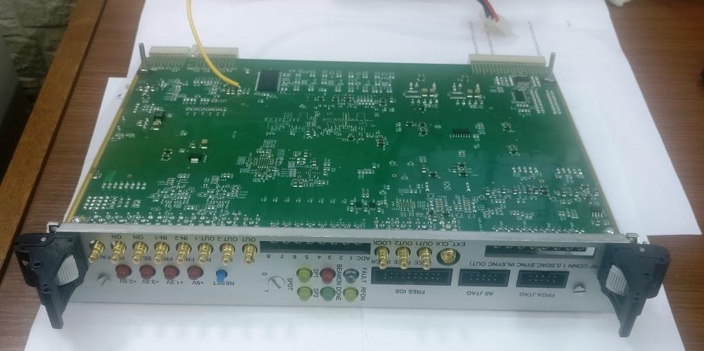
This board is a compact PCI based 6U board. This is a very high density, high speed multi-layer board consisting of the state of the art components such as high speed ADCs, DACs, high density, high speed FPGA, memories etc. with following interfaces:-
Analog to Digital Converters
- 14 bit, Octal ADC – 1 Nos.
- Sampling Speed – at least 70MHz with transformer ckt. for ADC drive with LVDS o/p
Digital to Analog Converters
- High speed 14 bit, dual channel Digital-to-Analog Converter – 2 Nos.
- Output update rate – at least 100MHz with transformer coupled output
- Supporting interleaved or non-interleaved modes using internal PLL
- Low speed 10 bit, dual channel Digital-to-Analog Converter – 3 Nos.
- DAC clock ~40MSPS (max) – from Clock generator
FPGA
- High speed, high density FPGA with at least 1,11,900 LAB
- JTAG Mode and Active Serial Mode – Using serial configuration device PROM for FPGA
CPCI 32 bit interface with burst transfer mode and interrupt capability.
Clock generation & distribution
- On board oscillator with around 80MHz LVCMOS oscillator
- ADC sampling clock of desired frequency (programmable with max. value of 100MHz) to be generated on board from external RF reference (sinusoidal) of 352MHz.
- CDCE62005 Clock generator devices may be used to provide clock inputs to the High speed ADCs, High speed DAC, Low speed (Debug) DAC, FPGA and Ref Out. – 2 Nos.
- Primary and secondary input selection for on board oscillator (80 MHz) or external RF Ref to generate ADC clock
- Supports LVPECL, LVDS or LVCMOS inputs and programmable output
SRAM interface:-
- 512Kx32bit Async SRAMS – 6 Nos.
- To be interfaced to the FPGA for Read/Write.
RF reference distribution:-
- Incoming RF Reference of 352MHz attenuated and fed to the clock generation and Reference ADC channel through transformer based drive circuit
Other interfaces:-
- Input connectors : Free in, Fault, Interlock, JTAG connection to be brought out on the front panel, one spare connector
- Output connectors : Sync_out, Free_out, Dbg_Out1, Dbg_out_2
- Front Panel : System reset (PB switch), SPDT switch, 32 Free IOs (2x20 Headers 0.1”), LEDs for important power supplies
- On PCB : 4 DIP switches, LEDs for other important signals on PCBs, LED for Configuration Done
- All connectors - Gold plated SMB
Subscribe Newsletter
A quick message to TECHNID
Client Speaks
Lorem Ipsum is simply dummy text of the printing and ty . . .
Lorem Ipsum is simply dummy text of the printing and ty . . .
Lorem Ipsum is simply dummy text of the printing and ty . . .
.jpg)
This board is a compact PCI based 6U board. This is a very high density, high speed multi-layer board consisting of the state of the art components such as high speed ADCs, DACs, high density, high speed FPGA, memories etc. with following interfaces:-
Analog to Digital Converters
- 14 bit, Octal ADC – 1 Nos.
- Sampling Speed – at least 70MHz with transformer ckt. for ADC drive with LVDS o/p
Digital to Analog Converters
- High speed 14 bit, dual channel Digital-to-Analog Converter – 2 Nos.
- Output update rate – at least 100MHz with transformer coupled output
- Supporting interleaved or non-interleaved modes using internal PLL
- Low speed 10 bit, dual channel Digital-to-Analog Converter – 3 Nos.
- DAC clock ~40MSPS (max) – from Clock generator
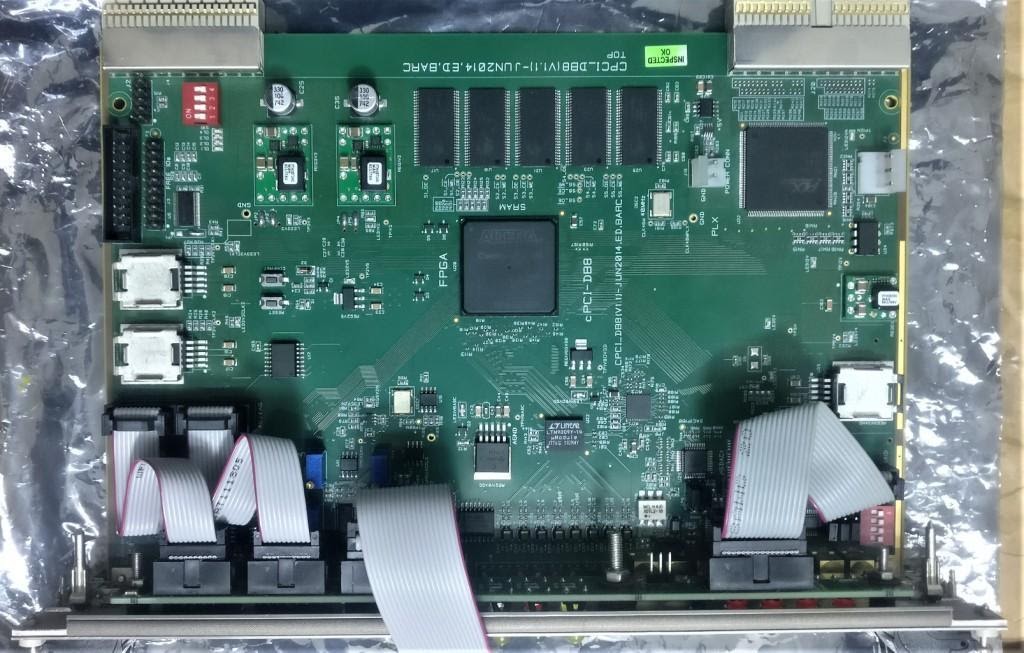
FPGA
- High speed, high density FPGA with at least 1,11,900 LAB
- JTAG Mode and Active Serial Mode – Using serial configuration device PROM for FPGA
CPCI 32 bit interface with burst transfer mode and interrupt capability.
Clock generation & distribution
- On board oscillator with around 80MHz LVCMOS oscillator
- ADC sampling clock of desired frequency (programmable with max. value of 100MHz) to be generated on board from external RF reference (sinusoidal) of 352MHz.
- CDCE62005 Clock generator devices may be used to provide clock inputs to the High speed ADCs, High speed DAC, Low speed (Debug) DAC, FPGA and Ref Out. – 2 Nos.
- Primary and secondary input selection for on board oscillator (80 MHz) or external RF Ref to generate ADC clock
- Supports LVPECL, LVDS or LVCMOS inputs and programmable output
SRAM interface:-
- 512Kx32bit Async SRAMS – 6 Nos.
- To be interfaced to the FPGA for Read/Write.
.jpg)
RF reference distribution:-
- Incoming RF Reference of 352MHz attenuated and fed to the clock generation and Reference ADC channel through transformer based drive circuit
Other interfaces:-
- Input connectors : Free in, Fault, Interlock, JTAG connection to be brought out on the front panel, one spare connector
- Output connectors : Sync_out, Free_out, Dbg_Out1, Dbg_out_2
- Front Panel : System reset (PB switch), SPDT switch, 32 Free IOs (2x20 Headers 0.1”), LEDs for important power supplies
- On PCB : 4 DIP switches, LEDs for other important signals on PCBs, LED for Configuration Done
- All connectors - Gold plated SMB