

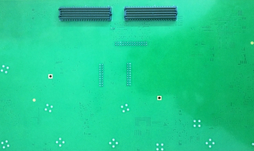
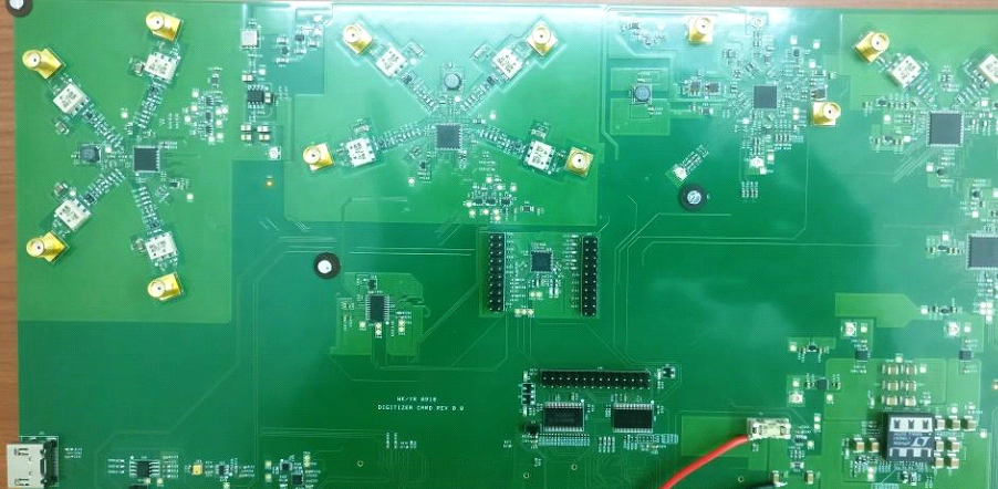
This is an ANSI VITA electrical compliant ADC-DAC Card having high channel to channel isolation and very high speed. This card also generates very low jitter, programmable frequency clock with programmable various IO standards. Following are the features of this card:-
Following are the main features of the product :-
- ADC section: Two nos. of Quad channel, 16 bit, 125MSPS, LVDS output, 600MHz Analog BW ADCs with transformer drive circuit for ADC input and with LVDS o/p. Reference through external circuit. SPI interface for internal register programming. ADC outputs and necessary control signals mapped to FPGA. The channel to channel isolation for the system is -70dbm.
- DAC section: Two high speed, 16 bit, dual channel DAC, 500MSPS with transformer coupled output, supporting SPI interface for internal register programming. DAC input and necessary control signals mapped to FPGA. One 10 bit, dual channel DAC, Clock ~40MSPS (max) with differential outputs and OPAMP for differential to single ended conversion followed by 5MHz RC LP filter DAC input and necessary control signals to be mapped to FPGA.
- Clock section: The board receives 1320MHz clock through the FMC and generates suitable clock signals for the ADCs and DACs using very low jitter clock divider and buffer. The division ratio is programmable through internal register of the clock divider IC via SPI. Supports bipolar sinusoidal, LVPECL, LVDS or LVCMOS inputs and programmable output.
- Power supply section: Analog and Digital power supply for the ADC section, DAC section, Clock section and supervisory section shall be generated in this section. The design should have suitable decoupling and noise filtering components to reduce the ripple and noise at the power supply outputs. The LDOs selected for providing power supply to the ADC should be very low noise.
- Using SFP, Card can act as White Rabbit Node using SYNCE and PTP in a large network.
- Supervisory section: Monitors the clock level, +12V & 3.3V power supplies, temperature at near the ADCs, DACs, Clock section and power supply sections. It also monitors vibration using accelerometer and micro phonic noise. It is facilitated by using SPI controlled ADC.
Applications:- Low Level RF Detection in Accelerator Control Application
Subscribe Newsletter
A quick message to TECHNID
Client Speaks
Lorem Ipsum is simply dummy text of the printing and ty . . .
Lorem Ipsum is simply dummy text of the printing and ty . . .
Lorem Ipsum is simply dummy text of the printing and ty . . .

Features
This is an ANSI VITA electrical compliant ADC-DAC Card having high channel to channel isolation and very high speed. This card also generates very low jitter, programmable frequency clock with programmable various IO standards. Following are the features of this card:-
- ADC section: Two nos. of Quad channel, 16 bit, 125MSPS, LVDS output, 600MHz Analog BW ADCs with transformer drive circuit for ADC input and with LVDS o/p. Reference through external circuit. SPI interface for internal register programming. ADC outputs and necessary control signals mapped to FPGA. The channel to channel isolation for the system is -70dbm.
- DAC section: Two high speed, 16 bit, dual channel DAC, 500MSPS with transformer coupled output, supporting SPI interface for internal register programming. DAC input and necessary control signals mapped to FPGA. One 10 bit, dual channel DAC, Clock ~40MSPS (max) with differential outputs and OPAMP for differential to single ended conversion followed by 5MHz RC LP filter DAC input and necessary control signals to be mapped to FPGA.
Features
- Clock section: The board receives 1320MHz clock through the FMC and generates suitable clock signals for the ADCs and DACs using very low jitter clock divider and buffer. The division ratio is programmable through internal register of the clock divider IC via SPI. Supports bipolar sinusoidal, LVPECL, LVDS or LVCMOS inputs and programmable output.
- Power supply section: Analog and Digital power supply for the ADC section, DAC section, Clock section and supervisory section shall be generated in this section. The design should have suitable decoupling and noise filtering components to reduce the ripple and noise at the power supply outputs. The LDOs selected for providing power supply to the ADC should be very low noise.
- Supervisory section: Monitors the clock level, +12V & 3.3V power supplies, temperature at near the ADCs, DACs, Clock section and power supply sections. It also monitors vibration using accelerometer and micro phonic noise. It is facilitated by using SPI controlled ADC.
Applications:- Low Level RF Detection in Accelerator Control Application